The Beginning of an End: 12 Years from the Hybrid Memory Cube to 3D-DRAM
There is a running theme in almost everything I have worked on: moving computation to where the data lives. The field has called it many things over the years, near-data processing (NDP), processing-in-memory (PIM), processing-near-memory (PNM), compute-in-memory (CIM), but the instinct behind all of them is the same. Transmitting data is expensive. Always has been. So push the compute toward the memory instead of dragging the memory toward the compute.
I started chasing this idea in earnest around 2014, at the beginning of my PhD. And this year, with our recent ISCA paper on a real 3D-DRAM accelerator, it finally shows up as product silicon. That should feel like a triumph, and in some ways it does. But it also feels like the beginning of an end, the closing of a line of research I have been circling for twelve years. This post is my personal perspective on that arc, from a research prototype almost nobody wanted to publish, to an industry that is now, all at once, moving in exactly this direction.
Where it started: the Hybrid Memory Cube
My first serious research was on Micron’s Hybrid Memory Cube (HMC). If you have never seen the inside of one, it is a small marvel: several DRAM dies stacked on top of a logic layer, connected vertically by through-silicon vias (TSVs), with the whole stack partitioned into vaults that each have their own controller. It was, quite literally, logic sitting underneath DRAM.
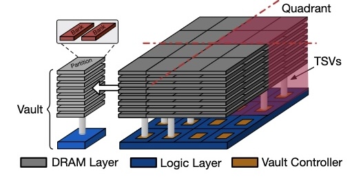
The internal structure of the 4 GB HMC 1.1 device we characterized: DRAM layers stacked over a logic layer, sliced into vaults and quadrants, stitched together with TSVs (IISWC'17).
We had a working HMC 1.1 prototype, which most of my directly related work is based on. I spent a lot of time simply measuring it, bandwidth, latency, temperature, and trying to reverse-engineer the internal network-on-chip that ties the vaults to the logic layer. This was not glamorous work, but it was honest: at the time, almost every PIM paper leaned on simulation, and there was real value in reporting what a physical stacked-memory part actually did. That characterization became our IISWC’17 paper, Demystifying the Characteristics of 3D-Stacked Memories.
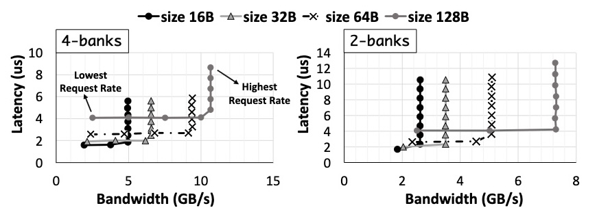
Measured latency versus achieved bandwidth on the real HMC, across request sizes (16–128 B) and access patterns. The "knee" where latency shoots up as you push toward peak bandwidth is the kind of thing you only learn from silicon, not simulation (IISWC'17, Fig. 17).
The idea I was betting on, together with my collaborators, was deliberately modest: change HMC as little as possible. Rather than redesigning memory around computation, we offloaded work at the instruction level, using the atomic operations HMC already exposed, and showed you could get real speedups with minimal disruption to the memory subsystem and its controller. That is GraphPIM (HPCA’17), which offloaded graph-framework operations with no changes to user code or the ISA, and CAIRO (TACO’17), a compiler-assisted framework that decides which instructions are actually worth offloading, so you get the wins without accidentally making things slower.
Two physical realities kept intruding on that clean picture, and both turned into papers. The first was the internal network. Latency inside the stack is not uniform; it depends on the NoC, on the access pattern, and on how loaded the vaults are.
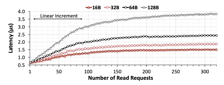
Average access latency as request pressure increases. Below the knee it climbs almost linearly; the larger the request size, the sooner the internal network starts to dominate (ISPASS'18, Fig. 8).
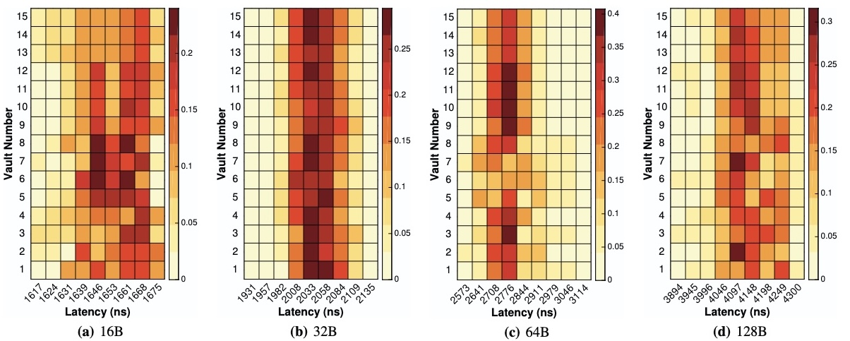
Per-vault latency distributions for different request sizes. The point is that "the latency" of a stacked memory is really a distribution shaped by the on-chip network, not a single number (ISPASS'18, Fig. 10).
We wrote those insights up as Performance Implications of NoCs on 3D-Stacked Memories (ISPASS’18). The second reality was heat. Stack logic under DRAM and run it hard, and you create hotspots on the logic layer that bleed up through the DRAM dies, exactly where you least want them. If you offload too aggressively, you cook the part.
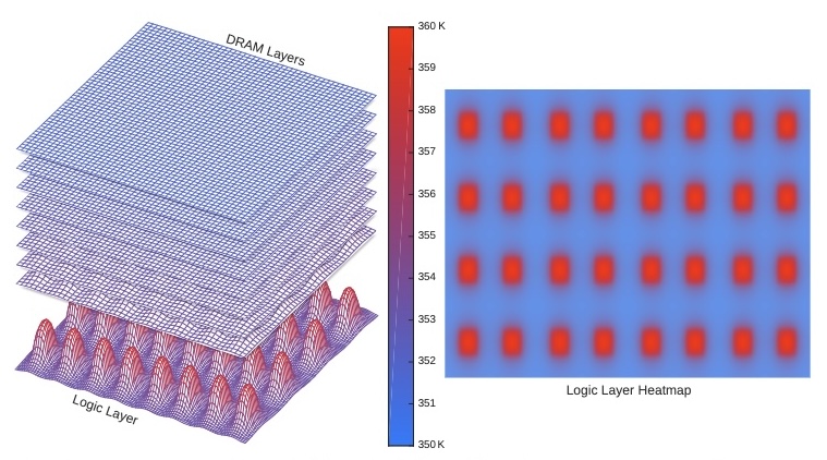
Thermal map of the stack under heavy utilization: the logic layer lights up with hotspots (~350–360 K) that conduct straight up into the DRAM. This is the thermal wall that motivated CoolPIM (IPDPS'18, Fig. 3).
That thermal wall is what CoolPIM (IPDPS’18) was about: thermally aware source throttling that dials PIM offloading up or down to stay inside the thermal budget while still coming out ahead. It is a small detail in the grand scheme, but I want to flag it now, because a decade later thermal reliability is still one of the hardest problems in stacking, and it shows up again at the very end of this story.
Why I walked away (and why it came back)
Here is the honest part. I moved off HMC as a primary focus, even though PIM/PNM/NDP stayed one of my core interests and quietly shows up in a lot of my later work. The reason was not that the ideas stopped being good. It was that the research community, at that moment, was largely against this line of work. Getting these papers in got harder and harder. A few good ones went through, mostly not ours, but the mood had turned. So I shifted my center of gravity to what became the heart of my thesis: the distribution of inference computation.
It helps to remember that PIM has a long history of being fashionable and then unfashionable. The concept goes back to “logic-in-memory” ideas in the 1970s; there was a serious academic wave in the 1990s (IRAM, EXECUBE, and their cousins) that never made it to product because the process technology and economics were not there; and then, around the time I started, 3D stacking triggered a third wave. HMC and HBM had finally made “a logic layer under DRAM” a manufacturable thing, and PIM came back to life. So when I say I was working on this in 2014, I was really joining the third act of a play that had already been staged twice before. Knowing that made the community’s skepticism easier to take, and, in hindsight, easier to disagree with.
The industry orbit: SK hynix, Rain AI, d-Matrix
After I graduated, I stayed in the gravitational field of processing-in-memory, even when I told myself I was doing something else.
My first job was at SK hynix. I took it largely because I wanted to learn about CMOS image sensors (CIS), but the project itself was about integrating intelligence into a 3D-stacked architecture built around an image sensor, essentially a smart, always-on sensor that could detect edges and run things like super-resolution close to where the pixels are captured. Compute next to the data again, just with photons on one end.
From there I joined Rain AI, which was doing processing-in-memory more or less head-on. That was where I got to watch, from inside industry, the ideas I had chased in research actually get built, though at that point everything still lived on a single die or across a few chiplets. What stuck with me was that in my last year there, we started seriously asking a different question: how do we stack? How do we put logic below the DRAM, or integrate with HBM in a smarter way? The vocabulary of my PhD was creeping back into the roadmap.
Rain didn’t pan out, and I joined d-Matrix. And this is where the pieces I had been carrying separately finally fell into one place. My thesis work was on distributing inference computation, which is exactly what you are forced to do on any reticle-limited die. My older life was 3D stacking. With our recent ISCA paper, both of those threads are now the same thread.
The payoff: Raptor and real 3D-DRAM
Our ISCA’26 paper, Early Silicon of Raptor: The First 3D-DRAM Accelerator for Generative Inference, is the concrete version of everything above: a logic die and a DRAM stack bonded together, with the logic sitting above the DRAM (as a prototype), running real generative models.
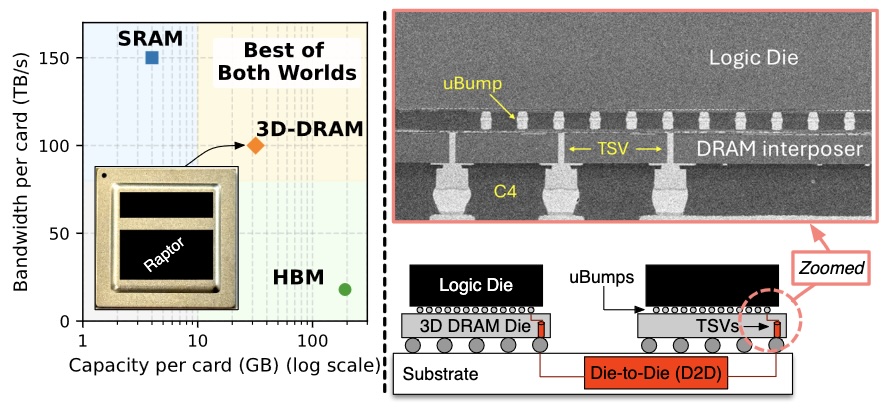
Left: the bandwidth–capacity trade-off. SRAM gives you bandwidth but not capacity; HBM gives you capacity but is bandwidth- and power-limited; 3D-DRAM aims for the "best of both worlds" corner. Right: an X-ray cross-section of Raptor's logic die face-to-face (F2F) bonded to the 3D-DRAM, with the µbump / TSV / C4 stack visible (ISCA'26, Fig. 1).
Generative inference is memory-bound. The prefill phase is compute-heavy, but decode, generating one token at a time, is dominated by reading and writing the growing key–value (KV) cache, and that traffic scales badly with model size and context length. On a Llama-70B model, the KV cache can grow from around 10 GB at batch 1 to hundreds of GB at larger batches, which is precisely the regime where memory bandwidth and capacity, not raw FLOPs, decide your throughput and your time-per-output-token.
What I like about the Raptor work is that it does not treat 3D-DRAM as an abstract idea; it deals with the ugly physical realities I remember from HMC. The paper introduces four architectural features to make 3D-DRAM actually practical: stream-blocking, which maps KV-cache streams onto configurable 3D-DRAM channels and sustains up to 100 TB/s per card while keeping bank-level parallelism; a pinless data-bus-inversion scheme (“stream-flipping”) over the single-cycle, wide face-to-face µbump interface that cuts I/O energy by about 18%; a topology-preserving redundancy scheme so that faulty banks can be bypassed without crippling channel width; and interleaved ECC with thermal-aware refresh for reliability at junction temperatures up to 105 °C. That last one made me smile, because it is CoolPIM’s thermal wall, ten years later, still standing guard. Built on a TSMC N4P logic die with 840 banks per DRAM die feeding tensor-engine slices, Raptor reports 4.71× and 2.44× higher throughput than HBM- and SRAM-based designs respectively, and 9.96× lower time-per-output-token than HBM-based designs, across a spread of models (Llama-3.1 70B, DeepSeek-V3, Kimi K2, GPT-OSS, Whisper, Canary).
But the single figure that captures the whole thesis is this one:
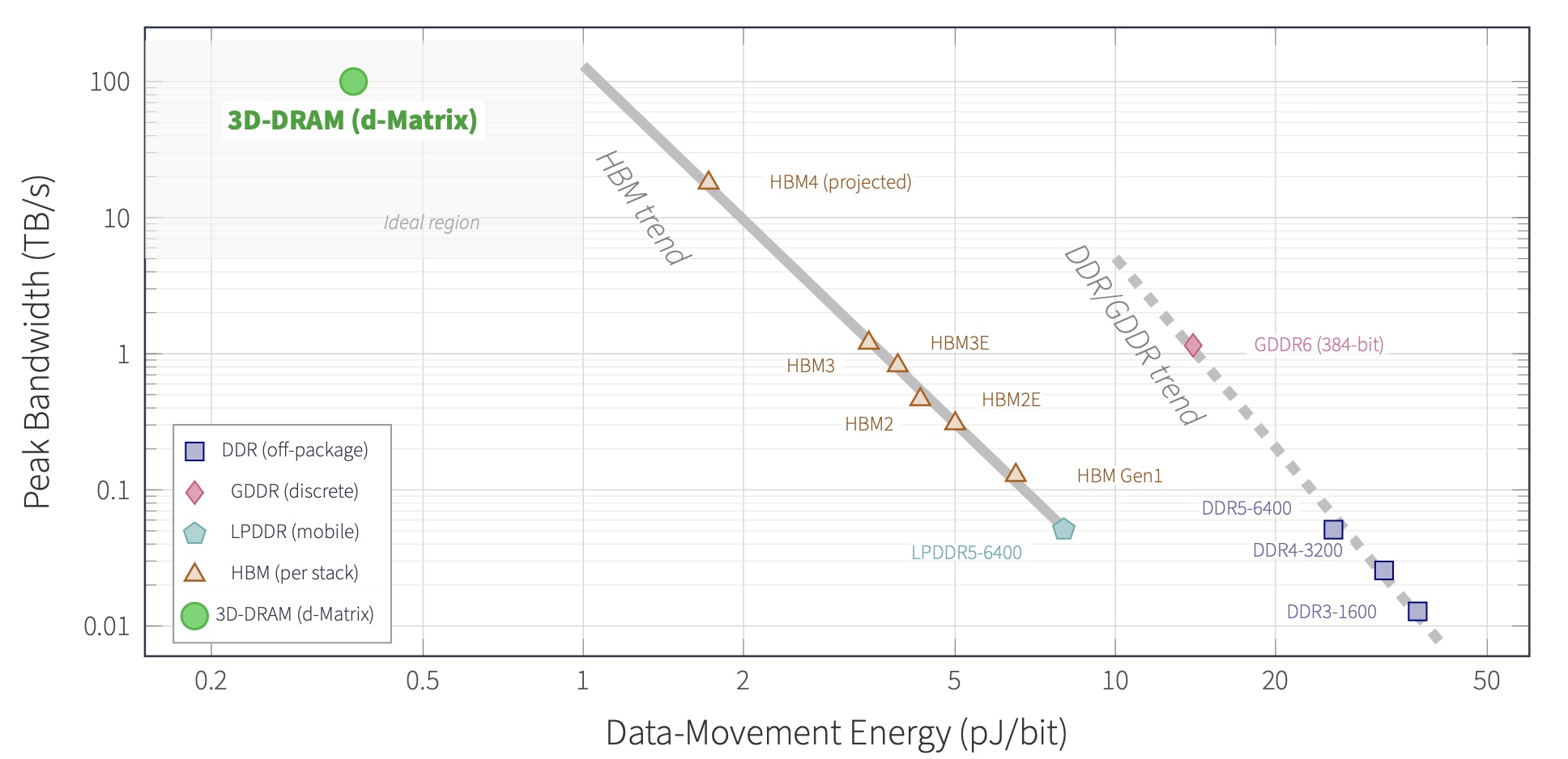
Peak bandwidth versus data-movement energy per bit. DDR, GDDR, and HBM all march along their trend lines, trading energy for bandwidth. 3D-DRAM sits alone in the top-left "ideal" corner: high bandwidth at low energy per bit. This is the entire argument for moving compute into memory, in one chart (ISCA'26, Fig. 3).
Moving a bit across a package costs energy, and for decode, where data movement dominates, that energy is the bottleneck. Put the compute under the DRAM and the bits barely have to travel. That is the whole game.
I am not alone in this anymore
The strangest part of publishing this now is that the industry has, more or less simultaneously, decided the same thing. For years “logic under DRAM” was a research position you had to defend. Today it is a roadmap that half the industry is racing down.
The clearest example is Qualcomm’s HBC (High-Bandwidth Compute), announced in mid-2026, which places a compute die directly beneath a stack of LPDDR DRAM connected by TSVs, and targets exactly the memory-bound decode phase of LLM inference, showing up on their AI250-class roadmap. (In an earlier draft of this post I called it “HCM / High Compute Memory” from memory; the real name is HBC, and the concept, cheap DRAM stacked over a compute die, is almost word-for-word the thing I was arguing for a decade ago.)
It is not just the newcomers. HBM4 moves the base die of the stack off a DRAM process and onto a logic foundry process, SK hynix’s HBM4 uses a TSMC logic base die, with custom base dies (C-HBM4E) heading toward 3 nm-class nodes, and NVIDIA is reported to be designing its own HBM base die around 2027. Read that again: the “logic layer under the DRAM” that made HMC special is now becoming the default way HBM is built. On the in-memory-compute side, SK Hynix’s AiM/AiMX and Samsung’s HBM-PIM (Aquabolt-XL) both put arithmetic units inside the memory to attack the same memory-bound GEMV that dominates decode. Different packages, same instinct.
And there is one more thread I will only touch here, because it is really its own story: offloading collective communication closer to the network and the memory, which is showing up in things like Meta’s MTIA 300 roadmap. That is the same instinct behind one of my co-authored papers, FAFNIR (HPCA’21), which does near-memory reduction as sparse data is gathered. I would like to write about collectives and in-network reduction properly in a future post; for now I will just note that it, too, fits under the same roof.
What it feels like to be one drop in the flood
So here is the feeling I actually wanted to write down. From a performance standpoint, none of this is surprising. Moving data is costly; pushing toward compute-in-memory was, in a sense, always the obvious answer. At Rain we used to talk about building something more like a brain, where memory is where compute happens. What changed is not the insight but the viability: 3D stacking is now a defensible technological choice rather than a research fantasy, and it is the natural next step of customization for higher performance. LLMs pushed it over the edge. You used to be able to get by with a somewhat faster, tightly integrated memory. Now you need enormous capacity, you need to distribute the computation well, collective communication and latency genuinely matter, and all of those pressures point the same way: toward processing near memory, in memory, using DRAM, near the data.
And yet, looking back, the thing I keep turning over is not the technology. It is what it means to have been one of the people who argued for a direction that turned out to be right. Because in research you have to start from an idea and build on it, and to do that you drift away from what is realistic today toward something imaginary, something the technology cannot yet support. If the direction is correct, then even when your specific papers go stale or turn out to be wrong in their details, the direction was right. That is a strange and genuinely interesting feeling: to be validated in aim while being obsolete in specifics.
But it also comes with a humbling correction. You are never the sole contributor. You are one drop in a flood of people all pushing on the same wall, adding to a shared pool of knowledge that, collectively, demonstrates a direction is viable, until eventually someone, or many someones, picks it up and carries it into reality. I don’t believe a single person, or a single company, ever really invents a new technology or a new idea. It emerges from a pool of people; it is, in the end, a humanity-scale effort. Assigning the credit to one name, one group, one logo, is almost always the wrong model of how any of this actually happened.
Which is why, when I say this might be the beginning of an end for a line of research I started in 2014, I mean it with more gratitude than sadness. The idea outgrew me, exactly as it was supposed to.
References
My papers referenced in this post
- GraphPIM: Enabling Instruction-Level PIM Offloading in Graph Computing Frameworks — L. Nai, R. Hadidi, J. Sim, H. Kim, P. Kumar, H. Kim. HPCA’17.
- CAIRO: A Compiler-Assisted Technique for Enabling Instruction-Level Offloading of Processing-In-Memory — R. Hadidi, L. Nai, H. Kim, H. Kim. ACM TACO’17.
- Demystifying the Characteristics of 3D-Stacked Memories: A Case Study for Hybrid Memory Cube — R. Hadidi, B. Asgari, B. A. Mudassar, S. Mukhopadhyay, S. Yalamanchili, H. Kim. IISWC’17.
- Performance Implications of NoCs on 3D-Stacked Memories: Insights from the Hybrid Memory Cube — R. Hadidi, B. Asgari, J. Young, B. A. Mudassar, K. Garg, T. Krishna, H. Kim. ISPASS’18.
- CoolPIM: Thermal-Aware Source Throttling for Efficient PIM Instruction Offloading — L. Nai, R. Hadidi, H. Xiao, H. Kim, J. Sim, H. Kim. IPDPS’18.
- FAFNIR: Accelerating Sparse Gathering by Using Efficient Near-Memory Intelligent Reduction — B. Asgari, R. Hadidi, J. Cao, D. E. Shim, S.-K. Lim, H. Kim. HPCA’21.
- Early Silicon of Raptor: The First 3D-DRAM Accelerator for Generative Inference — P. J. Nair, R. Hadidi, et al. ISCA’26.
A full list of my work is on my publications page.
Coverage of Raptor
- Kevin Quimbo, 3D-DRAM, explained — an independent, interactive plain-language visual guide to the paper, unaffiliated with the authors or d-Matrix.
- Silicon & Systems, Dropping the PHY: d-Matrix Bonds Compute Directly onto DRAM — technical analysis of the ISCA paper and Hot Chips presentation.
- ServeTheHome, d-Matrix Raptor 3D-DRAM Accelerator for Generative Inference at Hot Chips 2026 — a walkthrough of the Hot Chips presentation.
- Tom’s Hardware, Hot Chips 2026: d-Matrix stacks AI accelerator directly on custom DRAM for 100 TB/s per card — news analysis connecting the presentation with the ISCA paper.
- Wccftech, d-Matrix’s Raptor 3D DRAM Achieves SRAM-Class Bandwidth at 1/10th the HBM Power — a detailed architectural overview from Hot Chips.
- XenoSpectrum, d-Matrix’s Raptor Chip Hits 105 TB/s in Real Silicon Tests, But It’s Not an HBM Replacement Yet — analysis separating measured silicon results from modeled and product-level projections.
- Hardware Busters, d-Matrix Raptor Drops the Memory PHY: 32GB at 100 TB/s Against HBM4’s 192GB at 18 — coverage focused on the bandwidth, capacity, and energy trade-offs.
Other sources
- Qualcomm HBC (High-Bandwidth Compute) near-memory architecture and AI250/AI350 roadmap — Tom’s Hardware, Forbes.
- HBM4 logic base die (SK hynix on TSMC ~12 nm) and custom C-HBM4E on 3 nm-class nodes — TrendForce (C-HBM4E).
- NVIDIA reportedly designing its own HBM base die (~2027) — TrendForce.
- SK hynix AiM / GDDR6-AiM / AiMX accelerator card — SK hynix Newsroom.
- Samsung HBM-PIM (Aquabolt-XL) — IEEE (Hot Chips 2021).
- Meta MTIA 300 custom-silicon roadmap (collective offload near network/memory) — Meta Newsroom.
- d-Matrix 3D-stacked in-memory compute (3DIMC) — d-Matrix: Going Vertical.
- Micron Hybrid Memory Cube background — Hybrid Memory Cube (overview).
- History and waves of processing-in-memory — O. Mutlu et al., Processing Data Where It Makes Sense.
External performance figures above are as stated by their respective vendors/press and are not independent benchmarks; items marked “reported” are press reports, not official confirmations.