- 8-bit CPU: github.com/ramyadhadidi/tt06-8bit-cpu
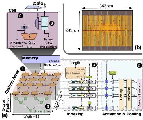
- 8-bit CIM: github.com/ramyadhadidi/tt07-8bit-vector-compute-in-SRAM
Taping Out ASICs: My First Hardware-Design Related Entry
My first programming languages were Assembly, Verilog, and C; not Python or Java. I have a bachelor’s degree in Electrical Engineering with a focus on digital systems, where I managed a microprocessor systems lab working with Altera and Xilinx FPGAs, microcontrollers, and processors. That foundation shaped how I think about computation: not as abstract instructions, but as signals propagating through gates, wires, and flip-flops. Training a workforce to write Python is relatively straightforward; training engineers who truly understand what happens beneath the abstraction layers, from transistor physics to RTL to microarchitecture, takes years of study and hands-on experimentation. That deeper understanding informs everything I do, including the software I write and the architectural decisions I make.
My daily work centers on computer architecture, my PhD training at Georgia Tech and beyond, focusing on extracting performance from custom hardware for workloads like deep neural networks and large language models. At d-Matrix (and before at Rain AI), I’m part of the team building the world’s first compute-in-memory (CIM) accelerator for ultra-low-latency LLM inference, so the gap between architecture-level design and physical implementation is something I encounter every day. Two things pushed me to close that gap further by getting hands-on with ASIC tapeouts:
- Bridging microarchitecture and silicon. Working at a hardware startup designing an accelerator, I wanted direct exposure to what comes after microarchitecture: synthesis, place-and-route, timing closure, and physical layout. Understanding these stages, even at a basic level, makes me a better architect.
- The hardware workforce problem. At a talk by Jason Cong (UCLA), he highlighted the stark shortage of hardware engineers relative to software engineers, a gap that the CHIPS Act aims to address but that remains difficult to close, especially for advanced nodes. The volatile geopolitical landscape around semiconductor manufacturing makes building domestic hardware expertise more urgent than ever.
Although several of my research papers include physical layouts and I have substantial FPGA experience from various projects and publications, I had never personally taped out an ASIC. TinyTapeout gave me the perfect opportunity: tape out a design on a 130nm open-source Skywater process (fabricated at a US-based facility), participate in a multi-project shuttle, and receive a packaged chip on a test board, all for a modest fee.
What is TinyTapeout? TinyTapeout is a platform that lets individuals tape out custom ASIC designs and receive them as packaged ICs mounted on a test board with an RP2040 Raspberry Pi Pico for control and I/O. It dramatically lowers the barrier to entry for chip design, you write your Verilog (or use their Wokwi graphical editor), push to GitHub, and their CI pipeline runs the full OpenLane synthesis, place-and-route, and DRC/LVS flow.
What is a Shuttle? Every IC contains a rectangular silicon die, which was once part of a round silicon wafer. Foundries typically sell wafer runs, where the same design is replicated hundreds of times across the wafer. For individuals and small teams, buying an entire wafer is cost-prohibitive, you only need one or two dies. A shuttle (or multi-project wafer, MPW) solves this by aggregating many different designs onto a single wafer, splitting the fabrication cost among participants. TinyTapeout acts as the shuttle organizer: you submit your design, and they handle tapeout logistics, die packaging (standard black plastic IC packages), and even provide the test board.
How Much Do These Designs Cost? The first design (1 tile) costs around $100. The second design (2×2 = 4 tiles) costs around $300. Remarkably affordable for real silicon.
What’s the Tile Size? 160 × 100 µm, small, but enough for meaningful digital designs at 130nm.
What’s the PDK? The open-source Skywater 130nm PDK (documentation), using the
sky130_fd_sc_hdstandard cell library. This is the same PDK used by Google’s open-source MPW shuttles and the broader open-silicon ecosystem.
8-bit Single-Cycle Microprocessor on TinyTapeout Shuttle 6
I submitted this design under the title “8-Bit CPU In a Week”, which is exactly what it was. The entire processor was designed, verified, and submitted in under a week, fitting into a single TinyTapeout tile. I reused and adapted portions of my 5-stage pipelined MIPS processor from 2013 (written during my undergraduate studies), but stripped it down to a single-cycle architecture to fit within the tile’s area constraints.
The processor features a 14-register register file and a full Arithmetic Logic Unit (ALU) with carry-flag tracking. I intentionally omitted memory operations (loads/stores to external memory) because managing the communication protocol with the RP2040 controller on the test board would have added significant complexity without much pedagogical value. Instead, I focused on a clean, self-contained datapath: instruction decode → register file read → ALU execute → register file write-back, all in a single clock cycle.
The design is implemented in a single Verilog file (~385 lines) with three internal modules: myCPU (top-level controller and datapath), RF1 (register file), and ALU1 (arithmetic logic unit). More details in the repo.
ISA Overview
The 4-bit opcode ISA is partitioned into register operations (opcodes 0x0–0x7) and ALU operations (opcodes 0x8–0xF):
- MVR (0x0): Move between registers
- LDB (0x1): Load immediate byte into register
- STB (0x2): Store register value to output
- RDS (0x3): Read processor status (ALU carry flag)
- NOT (0x8), AND (0x9), ORA (0xA), ADD (0xB), SUB (0xC), XOR (0xD), INC (0xE): ALU operations
- Unused opcodes function as NOPs, providing room for future ISA extensions
Layout and Statistics
| Utilisation (%) | Wire length (um) |
|---|---|
| 56.74 | 30920 |
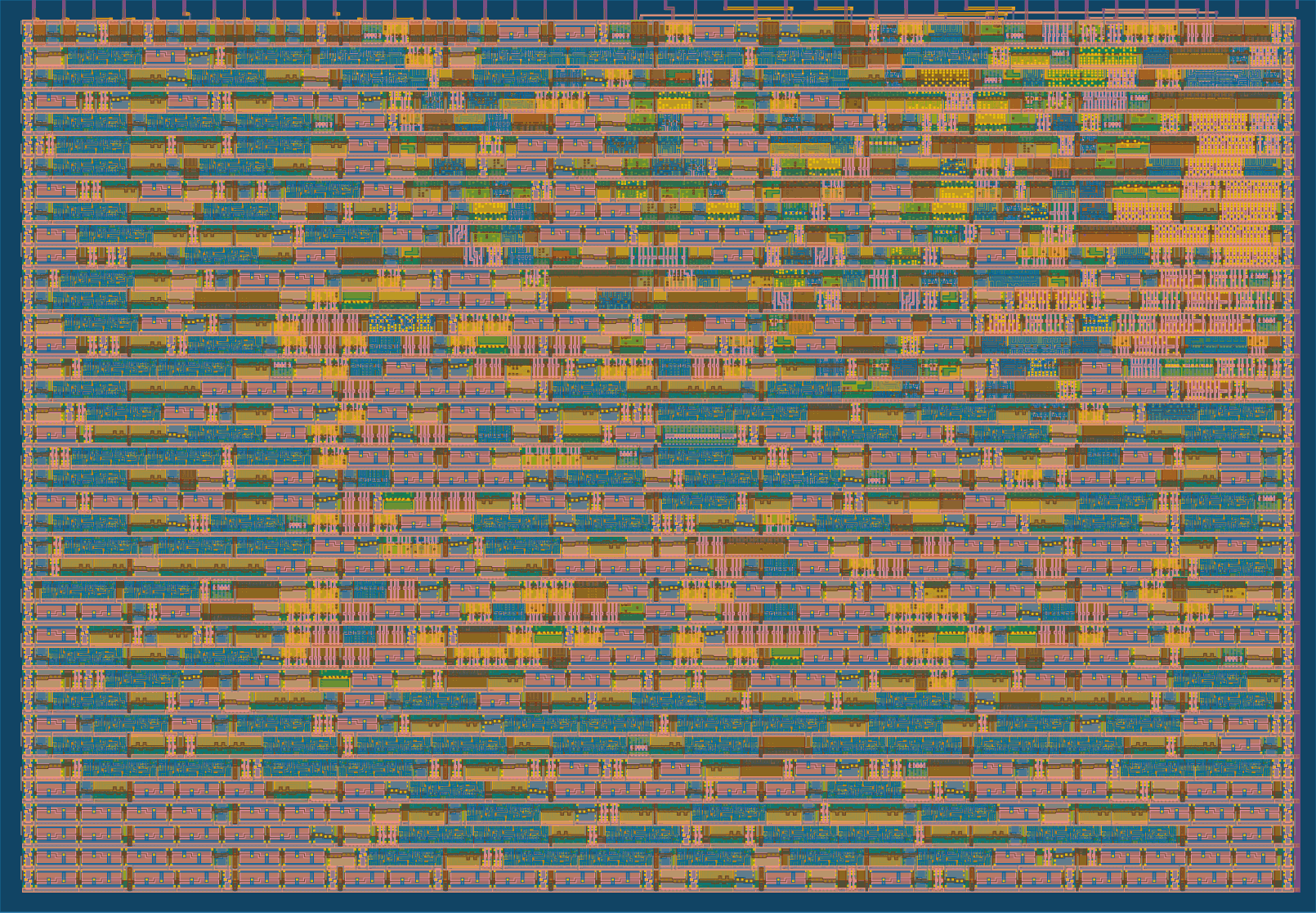
The design synthesized to 121 flip-flops (reflecting the 14×8-bit register file plus status registers), 119 multiplexers (for register selection), and 277 combinational logic cells, with a total utilization of 56.74% leaving comfortable routing headroom on the single tile.
Detailed Cell Breakdown (click to expand)
| Category | Cells | Count | |---------------|----------|-------| |Fill | [decap](https://skywater-pdk.readthedocs.io/en/main/contents/libraries/sky130_fd_sc_hd/cells/decap) [fill](https://skywater-pdk.readthedocs.io/en/main/contents/libraries/sky130_fd_sc_hd/cells/fill) | 1007| |Combo Logic | [and3b](https://skywater-pdk.readthedocs.io/en/main/contents/libraries/sky130_fd_sc_hd/cells/and3b) [a21oi](https://skywater-pdk.readthedocs.io/en/main/contents/libraries/sky130_fd_sc_hd/cells/a21oi) [a31oi](https://skywater-pdk.readthedocs.io/en/main/contents/libraries/sky130_fd_sc_hd/cells/a31oi) [and4b](https://skywater-pdk.readthedocs.io/en/main/contents/libraries/sky130_fd_sc_hd/cells/and4b) [a22o](https://skywater-pdk.readthedocs.io/en/main/contents/libraries/sky130_fd_sc_hd/cells/a22o) [a221o](https://skywater-pdk.readthedocs.io/en/main/contents/libraries/sky130_fd_sc_hd/cells/a221o) [and4bb](https://skywater-pdk.readthedocs.io/en/main/contents/libraries/sky130_fd_sc_hd/cells/and4bb) [a31o](https://skywater-pdk.readthedocs.io/en/main/contents/libraries/sky130_fd_sc_hd/cells/a31o) [a2111o](https://skywater-pdk.readthedocs.io/en/main/contents/libraries/sky130_fd_sc_hd/cells/a2111o) [o21a](https://skywater-pdk.readthedocs.io/en/main/contents/libraries/sky130_fd_sc_hd/cells/o21a) [nand3b](https://skywater-pdk.readthedocs.io/en/main/contents/libraries/sky130_fd_sc_hd/cells/nand3b) [a21o](https://skywater-pdk.readthedocs.io/en/main/contents/libraries/sky130_fd_sc_hd/cells/a21o) [a211oi](https://skywater-pdk.readthedocs.io/en/main/contents/libraries/sky130_fd_sc_hd/cells/a211oi) [or3b](https://skywater-pdk.readthedocs.io/en/main/contents/libraries/sky130_fd_sc_hd/cells/or3b) [o21ai](https://skywater-pdk.readthedocs.io/en/main/contents/libraries/sky130_fd_sc_hd/cells/o21ai) [o211a](https://skywater-pdk.readthedocs.io/en/main/contents/libraries/sky130_fd_sc_hd/cells/o211a) [o22a](https://skywater-pdk.readthedocs.io/en/main/contents/libraries/sky130_fd_sc_hd/cells/o22a) [o2bb2a](https://skywater-pdk.readthedocs.io/en/main/contents/libraries/sky130_fd_sc_hd/cells/o2bb2a) [a2111oi](https://skywater-pdk.readthedocs.io/en/main/contents/libraries/sky130_fd_sc_hd/cells/a2111oi) [a32o](https://skywater-pdk.readthedocs.io/en/main/contents/libraries/sky130_fd_sc_hd/cells/a32o) [a22oi](https://skywater-pdk.readthedocs.io/en/main/contents/libraries/sky130_fd_sc_hd/cells/a22oi) [o31a](https://skywater-pdk.readthedocs.io/en/main/contents/libraries/sky130_fd_sc_hd/cells/o31a) [or2b](https://skywater-pdk.readthedocs.io/en/main/contents/libraries/sky130_fd_sc_hd/cells/or2b) [a21bo](https://skywater-pdk.readthedocs.io/en/main/contents/libraries/sky130_fd_sc_hd/cells/a21bo) [o32a](https://skywater-pdk.readthedocs.io/en/main/contents/libraries/sky130_fd_sc_hd/cells/o32a) [a2bb2o](https://skywater-pdk.readthedocs.io/en/main/contents/libraries/sky130_fd_sc_hd/cells/a2bb2o) [o311a](https://skywater-pdk.readthedocs.io/en/main/contents/libraries/sky130_fd_sc_hd/cells/o311a) [and2b](https://skywater-pdk.readthedocs.io/en/main/contents/libraries/sky130_fd_sc_hd/cells/and2b) [a311o](https://skywater-pdk.readthedocs.io/en/main/contents/libraries/sky130_fd_sc_hd/cells/a311o) [nor2b](https://skywater-pdk.readthedocs.io/en/main/contents/libraries/sky130_fd_sc_hd/cells/nor2b) [o21ba](https://skywater-pdk.readthedocs.io/en/main/contents/libraries/sky130_fd_sc_hd/cells/o21ba) [o22ai](https://skywater-pdk.readthedocs.io/en/main/contents/libraries/sky130_fd_sc_hd/cells/o22ai) [o221a](https://skywater-pdk.readthedocs.io/en/main/contents/libraries/sky130_fd_sc_hd/cells/o221a) [o211ai](https://skywater-pdk.readthedocs.io/en/main/contents/libraries/sky130_fd_sc_hd/cells/o211ai) [o21bai](https://skywater-pdk.readthedocs.io/en/main/contents/libraries/sky130_fd_sc_hd/cells/o21bai) [a211o](https://skywater-pdk.readthedocs.io/en/main/contents/libraries/sky130_fd_sc_hd/cells/a211o) [o2111a](https://skywater-pdk.readthedocs.io/en/main/contents/libraries/sky130_fd_sc_hd/cells/o2111a) [a221oi](https://skywater-pdk.readthedocs.io/en/main/contents/libraries/sky130_fd_sc_hd/cells/a221oi) | 277| |Tap | [tapvpwrvgnd](https://skywater-pdk.readthedocs.io/en/main/contents/libraries/sky130_fd_sc_hd/cells/tapvpwrvgnd) | 225| |Buffer | [buf](https://skywater-pdk.readthedocs.io/en/main/contents/libraries/sky130_fd_sc_hd/cells/buf) [clkbuf](https://skywater-pdk.readthedocs.io/en/main/contents/libraries/sky130_fd_sc_hd/cells/clkbuf) | 197| |Flip Flops | [dfrtp](https://skywater-pdk.readthedocs.io/en/main/contents/libraries/sky130_fd_sc_hd/cells/dfrtp) | 121| |Multiplexer | [mux2](https://skywater-pdk.readthedocs.io/en/main/contents/libraries/sky130_fd_sc_hd/cells/mux2) | 119| |AND | [and2](https://skywater-pdk.readthedocs.io/en/main/contents/libraries/sky130_fd_sc_hd/cells/and2) [and4](https://skywater-pdk.readthedocs.io/en/main/contents/libraries/sky130_fd_sc_hd/cells/and4) [and3](https://skywater-pdk.readthedocs.io/en/main/contents/libraries/sky130_fd_sc_hd/cells/and3) | 38| |NAND | [nand2](https://skywater-pdk.readthedocs.io/en/main/contents/libraries/sky130_fd_sc_hd/cells/nand2) [nand3](https://skywater-pdk.readthedocs.io/en/main/contents/libraries/sky130_fd_sc_hd/cells/nand3) [nand2b](https://skywater-pdk.readthedocs.io/en/main/contents/libraries/sky130_fd_sc_hd/cells/nand2b) | 34| |NOR | [nor2](https://skywater-pdk.readthedocs.io/en/main/contents/libraries/sky130_fd_sc_hd/cells/nor2) [nor4](https://skywater-pdk.readthedocs.io/en/main/contents/libraries/sky130_fd_sc_hd/cells/nor4) [nor3](https://skywater-pdk.readthedocs.io/en/main/contents/libraries/sky130_fd_sc_hd/cells/nor3) [xnor2](https://skywater-pdk.readthedocs.io/en/main/contents/libraries/sky130_fd_sc_hd/cells/xnor2) | 32| |OR | [or3](https://skywater-pdk.readthedocs.io/en/main/contents/libraries/sky130_fd_sc_hd/cells/or3) [or2](https://skywater-pdk.readthedocs.io/en/main/contents/libraries/sky130_fd_sc_hd/cells/or2) [or4](https://skywater-pdk.readthedocs.io/en/main/contents/libraries/sky130_fd_sc_hd/cells/or4) [xor2](https://skywater-pdk.readthedocs.io/en/main/contents/libraries/sky130_fd_sc_hd/cells/xor2) | 29| |Misc | [dlygate4sd3](https://skywater-pdk.readthedocs.io/en/main/contents/libraries/sky130_fd_sc_hd/cells/dlygate4sd3) [dlymetal6s2s](https://skywater-pdk.readthedocs.io/en/main/contents/libraries/sky130_fd_sc_hd/cells/dlymetal6s2s) [conb](https://skywater-pdk.readthedocs.io/en/main/contents/libraries/sky130_fd_sc_hd/cells/conb) | 21| |Inverter | [inv](https://skywater-pdk.readthedocs.io/en/main/contents/libraries/sky130_fd_sc_hd/cells/inv) | 11| |Clock | [clkinv](https://skywater-pdk.readthedocs.io/en/main/contents/libraries/sky130_fd_sc_hd/cells/clkinv) | 1|More details in this action.
TinyTapeout Shuttle 7: 8-bit Vector Compute in SRAM Multiplier
This project is a vector dot-product accelerator with stationary weights, implemented on 4 tiles (2×2) in TinyTapeout. The entire design, Verilog, testbenches, and documentation, was completed in roughly 10 hours, broken down as: ~2 hours for a single MAC unit, ~2 hours for multi-MAC loading logic, ~1 hour for the adder tree, and ~2 hours for the readout circuit plus remaining documentation. To my surprise, this second project went much faster than the CPU, partly because the external interface was simpler (just 4 opcodes: LOAD_W, LOAD_A, READ_S, NOP), and partly because the design is more regular and repetitive. More details in the repo.
The design implements a weight-stationary dataflow: weights are loaded once into registers and reused across multiple activation vectors, minimizing data movement, exactly the pattern that dominates inference in transformer-based models. This compute paradigm is broadly termed processing in/near memory (PIM/PNM) or Compute in Memory (CIM). It’s not a new concept, I was actively publishing in this space starting in 2017, which was arguably the third wave of PIM interest:
- CAIRO (TACO’17): A compiler-assisted technique for instruction-level PIM offloading
- GraphPIM (HPCA’17): Enabling PIM offloading in graph computing frameworks
- HMC Characterization (IISWC’17): Demystifying 3D-stacked memory characteristics
- CoolPIM (IPDPS’18): Thermal-aware PIM instruction offloading
- FAFNIR (HPCA’21): Near-memory intelligent reduction for sparse gathering
However, I believe this paradigm is now here to stay. The memory-bound nature of LLM inference, where arithmetic intensity is low and data movement dominates energy and latency, makes CIM architectures not just academically interesting but commercially viable. This is, in fact, central to what d-Matrix or Rain AI are building.
Components and Operation
- MAC Units (×8): Each unit contains two 8-bit registers (one for weight W, one for activation A) and produces a 16-bit multiplication result. The stationary weight stays loaded while activations stream through.
- Adder Tree (3 levels): Level 1 pairs the 8 MAC outputs into 4 sums; Level 2 reduces to 2 sums; Level 3 produces the final 19-bit dot-product result, preserving full precision with no overflow. The adders use a Kogge-Stone carry-lookahead topology, which provides O(log n) carry propagation delay at the cost of additional area, a worthwhile tradeoff when latency matters.
- Readout Mechanism: Since the output interface is limited to 8 bits, the 19-bit result is read out over three sequential clock cycles (MSB-first), controlled by a cache-and-shift mechanism.
Layout and Statistics
| Utilisation (%) | Wire length (um) |
|---|---|
| 54.15 | 91602 |
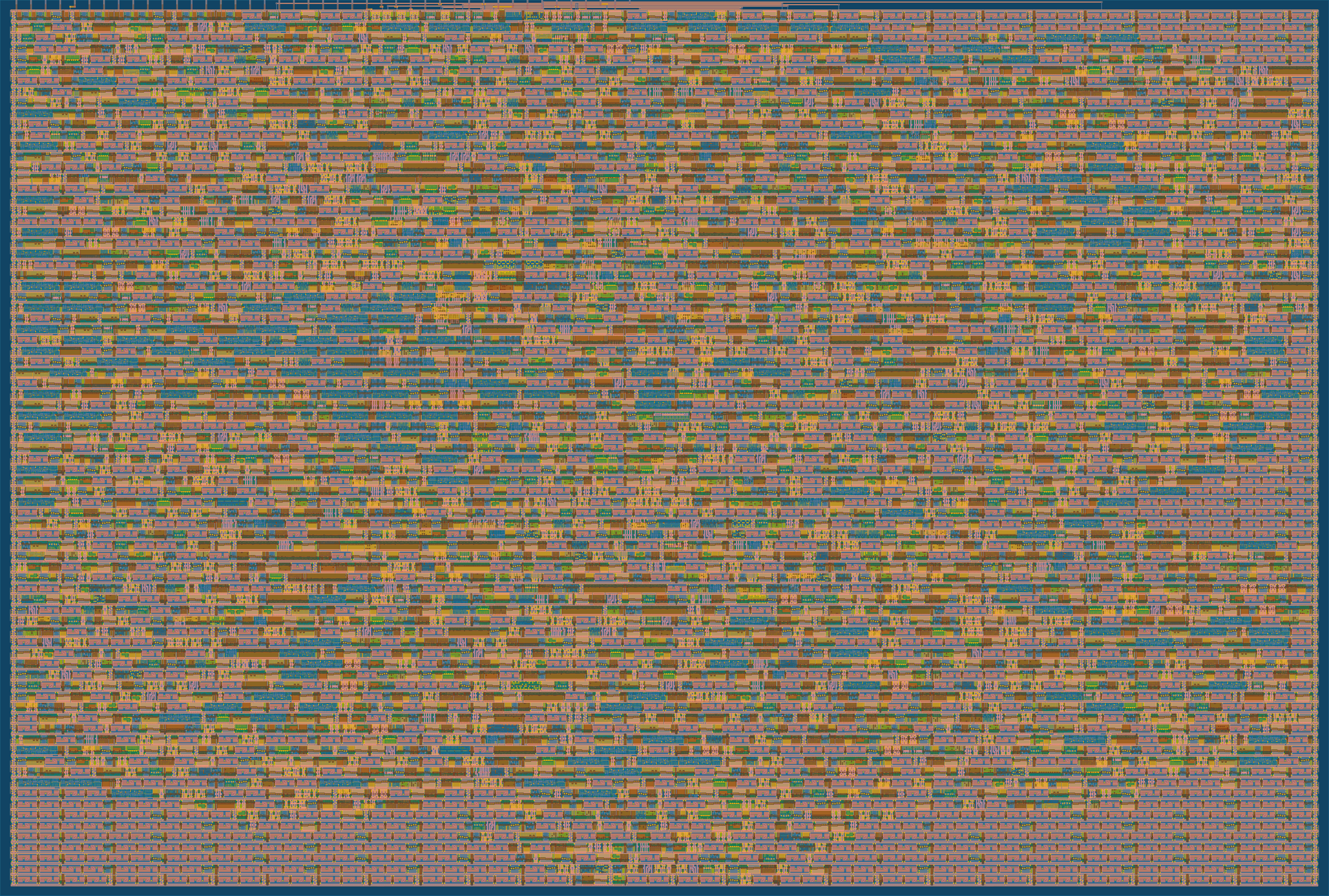
Compared to the CPU design, the CIM multiplier is substantially larger: 158 flip-flops (8×2 weight/activation registers plus control state), 1,291 combinational logic cells (dominated by the multiplier arrays and Kogge-Stone adders), and 3× the wire length (91,602 µm vs. 30,920 µm), yet it achieves a comparable utilization of 54.15% across the 4 tiles, indicating efficient use of the expanded area.
Detailed Cell Breakdown (click to expand)
| Category | Cells | Count | |---------------|----------|-------| |Fill | [decap](https://skywater-pdk.readthedocs.io/en/main/contents/libraries/sky130_fd_sc_hd/cells/decap) [fill](https://skywater-pdk.readthedocs.io/en/main/contents/libraries/sky130_fd_sc_hd/cells/fill) | 5412| |Combo Logic | [o21ai](https://skywater-pdk.readthedocs.io/en/main/contents/libraries/sky130_fd_sc_hd/cells/o21ai) [a22oi](https://skywater-pdk.readthedocs.io/en/main/contents/libraries/sky130_fd_sc_hd/cells/a22oi) [o2bb2a](https://skywater-pdk.readthedocs.io/en/main/contents/libraries/sky130_fd_sc_hd/cells/o2bb2a) [and2b](https://skywater-pdk.readthedocs.io/en/main/contents/libraries/sky130_fd_sc_hd/cells/and2b) [o21bai](https://skywater-pdk.readthedocs.io/en/main/contents/libraries/sky130_fd_sc_hd/cells/o21bai) [a21o](https://skywater-pdk.readthedocs.io/en/main/contents/libraries/sky130_fd_sc_hd/cells/a21o) [a22o](https://skywater-pdk.readthedocs.io/en/main/contents/libraries/sky130_fd_sc_hd/cells/a22o) [a32o](https://skywater-pdk.readthedocs.io/en/main/contents/libraries/sky130_fd_sc_hd/cells/a32o) [o21ba](https://skywater-pdk.readthedocs.io/en/main/contents/libraries/sky130_fd_sc_hd/cells/o21ba) [o21a](https://skywater-pdk.readthedocs.io/en/main/contents/libraries/sky130_fd_sc_hd/cells/o21a) [or3b](https://skywater-pdk.readthedocs.io/en/main/contents/libraries/sky130_fd_sc_hd/cells/or3b) [or2b](https://skywater-pdk.readthedocs.io/en/main/contents/libraries/sky130_fd_sc_hd/cells/or2b) [a21bo](https://skywater-pdk.readthedocs.io/en/main/contents/libraries/sky130_fd_sc_hd/cells/a21bo) [a31o](https://skywater-pdk.readthedocs.io/en/main/contents/libraries/sky130_fd_sc_hd/cells/a31o) [a21oi](https://skywater-pdk.readthedocs.io/en/main/contents/libraries/sky130_fd_sc_hd/cells/a21oi) [a31oi](https://skywater-pdk.readthedocs.io/en/main/contents/libraries/sky130_fd_sc_hd/cells/a31oi) [o211a](https://skywater-pdk.readthedocs.io/en/main/contents/libraries/sky130_fd_sc_hd/cells/o211a) [a211oi](https://skywater-pdk.readthedocs.io/en/main/contents/libraries/sky130_fd_sc_hd/cells/a211oi) [o211ai](https://skywater-pdk.readthedocs.io/en/main/contents/libraries/sky130_fd_sc_hd/cells/o211ai) [a211o](https://skywater-pdk.readthedocs.io/en/main/contents/libraries/sky130_fd_sc_hd/cells/a211o) [nand3b](https://skywater-pdk.readthedocs.io/en/main/contents/libraries/sky130_fd_sc_hd/cells/nand3b) [o22ai](https://skywater-pdk.readthedocs.io/en/main/contents/libraries/sky130_fd_sc_hd/cells/o22ai) [a311o](https://skywater-pdk.readthedocs.io/en/main/contents/libraries/sky130_fd_sc_hd/cells/a311o) [nand4b](https://skywater-pdk.readthedocs.io/en/main/contents/libraries/sky130_fd_sc_hd/cells/nand4b) [or4bb](https://skywater-pdk.readthedocs.io/en/main/contents/libraries/sky130_fd_sc_hd/cells/or4bb) [o31a](https://skywater-pdk.readthedocs.io/en/main/contents/libraries/sky130_fd_sc_hd/cells/o31a) [o32a](https://skywater-pdk.readthedocs.io/en/main/contents/libraries/sky130_fd_sc_hd/cells/o32a) [and4b](https://skywater-pdk.readthedocs.io/en/main/contents/libraries/sky130_fd_sc_hd/cells/and4b) [o22a](https://skywater-pdk.readthedocs.io/en/main/contents/libraries/sky130_fd_sc_hd/cells/o22a) [o311a](https://skywater-pdk.readthedocs.io/en/main/contents/libraries/sky130_fd_sc_hd/cells/o311a) [or4b](https://skywater-pdk.readthedocs.io/en/main/contents/libraries/sky130_fd_sc_hd/cells/or4b) [a41o](https://skywater-pdk.readthedocs.io/en/main/contents/libraries/sky130_fd_sc_hd/cells/a41o) [o31ai](https://skywater-pdk.readthedocs.io/en/main/contents/libraries/sky130_fd_sc_hd/cells/o31ai) [and4bb](https://skywater-pdk.readthedocs.io/en/main/contents/libraries/sky130_fd_sc_hd/cells/and4bb) [a2bb2oi](https://skywater-pdk.readthedocs.io/en/main/contents/libraries/sky130_fd_sc_hd/cells/a2bb2oi) [a2111o](https://skywater-pdk.readthedocs.io/en/main/contents/libraries/sky130_fd_sc_hd/cells/a2111o) [and3b](https://skywater-pdk.readthedocs.io/en/main/contents/libraries/sky130_fd_sc_hd/cells/and3b) [nor3b](https://skywater-pdk.readthedocs.io/en/main/contents/libraries/sky130_fd_sc_hd/cells/nor3b) [a2bb2o](https://skywater-pdk.readthedocs.io/en/main/contents/libraries/sky130_fd_sc_hd/cells/a2bb2o) [o2bb2ai](https://skywater-pdk.readthedocs.io/en/main/contents/libraries/sky130_fd_sc_hd/cells/o2bb2ai) [o2111a](https://skywater-pdk.readthedocs.io/en/main/contents/libraries/sky130_fd_sc_hd/cells/o2111a) [a221oi](https://skywater-pdk.readthedocs.io/en/main/contents/libraries/sky130_fd_sc_hd/cells/a221oi) [nor4b](https://skywater-pdk.readthedocs.io/en/main/contents/libraries/sky130_fd_sc_hd/cells/nor4b) [a2111oi](https://skywater-pdk.readthedocs.io/en/main/contents/libraries/sky130_fd_sc_hd/cells/a2111oi) [nor2b](https://skywater-pdk.readthedocs.io/en/main/contents/libraries/sky130_fd_sc_hd/cells/nor2b) [a221o](https://skywater-pdk.readthedocs.io/en/main/contents/libraries/sky130_fd_sc_hd/cells/a221o) | 1291| |Tap | [tapvpwrvgnd](https://skywater-pdk.readthedocs.io/en/main/contents/libraries/sky130_fd_sc_hd/cells/tapvpwrvgnd) | 1037| |NOR | [xnor2](https://skywater-pdk.readthedocs.io/en/main/contents/libraries/sky130_fd_sc_hd/cells/xnor2) [nor2](https://skywater-pdk.readthedocs.io/en/main/contents/libraries/sky130_fd_sc_hd/cells/nor2) [nor3](https://skywater-pdk.readthedocs.io/en/main/contents/libraries/sky130_fd_sc_hd/cells/nor3) [nor4](https://skywater-pdk.readthedocs.io/en/main/contents/libraries/sky130_fd_sc_hd/cells/nor4) | 629| |NAND | [nand2b](https://skywater-pdk.readthedocs.io/en/main/contents/libraries/sky130_fd_sc_hd/cells/nand2b) [nand2](https://skywater-pdk.readthedocs.io/en/main/contents/libraries/sky130_fd_sc_hd/cells/nand2) [nand3](https://skywater-pdk.readthedocs.io/en/main/contents/libraries/sky130_fd_sc_hd/cells/nand3) [nand4](https://skywater-pdk.readthedocs.io/en/main/contents/libraries/sky130_fd_sc_hd/cells/nand4) | 510| |AND | [and4](https://skywater-pdk.readthedocs.io/en/main/contents/libraries/sky130_fd_sc_hd/cells/and4) [and3](https://skywater-pdk.readthedocs.io/en/main/contents/libraries/sky130_fd_sc_hd/cells/and3) [and2](https://skywater-pdk.readthedocs.io/en/main/contents/libraries/sky130_fd_sc_hd/cells/and2) [a21boi](https://skywater-pdk.readthedocs.io/en/main/contents/libraries/sky130_fd_sc_hd/cells/a21boi) | 442| |Buffer | [buf](https://skywater-pdk.readthedocs.io/en/main/contents/libraries/sky130_fd_sc_hd/cells/buf) [clkbuf](https://skywater-pdk.readthedocs.io/en/main/contents/libraries/sky130_fd_sc_hd/cells/clkbuf) | 353| |OR | [or2](https://skywater-pdk.readthedocs.io/en/main/contents/libraries/sky130_fd_sc_hd/cells/or2) [or4](https://skywater-pdk.readthedocs.io/en/main/contents/libraries/sky130_fd_sc_hd/cells/or4) [xor2](https://skywater-pdk.readthedocs.io/en/main/contents/libraries/sky130_fd_sc_hd/cells/xor2) [or3](https://skywater-pdk.readthedocs.io/en/main/contents/libraries/sky130_fd_sc_hd/cells/or3) | 331| |Flip Flops | [dfrtp](https://skywater-pdk.readthedocs.io/en/main/contents/libraries/sky130_fd_sc_hd/cells/dfrtp) | 158| |Multiplexer | [mux2](https://skywater-pdk.readthedocs.io/en/main/contents/libraries/sky130_fd_sc_hd/cells/mux2) | 145| |Inverter | [inv](https://skywater-pdk.readthedocs.io/en/main/contents/libraries/sky130_fd_sc_hd/cells/inv) | 45| |Misc | [dlymetal6s2s](https://skywater-pdk.readthedocs.io/en/main/contents/libraries/sky130_fd_sc_hd/cells/dlymetal6s2s) [dlygate4sd3](https://skywater-pdk.readthedocs.io/en/main/contents/libraries/sky130_fd_sc_hd/cells/dlygate4sd3) [conb](https://skywater-pdk.readthedocs.io/en/main/contents/libraries/sky130_fd_sc_hd/cells/conb) | 43| |Diode | [diode](https://skywater-pdk.readthedocs.io/en/main/contents/libraries/sky130_fd_sc_hd/cells/diode) | 21|More details in this action.
Testing & Verification
One of the most underappreciated aspects of hardware design is verification. Unlike software, where you can step through code sequentially, Verilog describes hardware that operates inherently in parallel, every always block, every assign statement runs concurrently. Debugging requires thinking in terms of waveforms and timing diagrams rather than stack traces. Most of my development time on both projects was spent on verification, not design.
Both projects use cocotb (Coroutine-based Co-simulation Testbench) for verification. Cocotb lets you write testbenches in Python that drive and observe your Verilog design’s I/O ports through a simulator. This is enormously productive compared to writing traditional Verilog testbenches, you get Python’s full standard library, assertion framework, and the ability to generate randomized test vectors programmatically.
One practical limitation: TinyTapeout’s CI pipeline compiles the design as a black box, meaning testbenches can only access external pins (the ui_in, uo_out, and uio ports). Any tests that probe internal signals (register file contents, ALU intermediate values, etc.) must be run locally and are commented out in the committed test files. This is a real engineering constraint, you’re testing your chip the way you’d test real silicon, through its pins only.
Testing the 8-bit Single-Cycle Microprocessor
The processor was validated through 12 testbenches covering: LDB (load immediate), STB (store to output), all ALU operations (XOR, AND, ORA, ADD, SUB, INC), carry flag propagation, RDS (read status), and register-to-register moves. Each test loads operands into registers, executes an instruction, and checks the output pins against expected values.
Although basic operational correctness is verified, I intentionally did not exhaustively test inter-instruction timing hazards. In a single-cycle design without pipelining, data hazards don’t exist in the traditional sense, but the interface timing with the RP2040 controller introduces its own synchronization considerations. A proper compiler or assembler would handle these, much like early MIPS compilers inserted NOPs to manage pipeline hazards. View the full test suite here.
Testing the Compute in SRAM Multiplier
The CIM design has a more extensive verification suite (~1,300 lines of Python), organized into four progressive categories that mirror how I built the design bottom-up:
- Single MAC Operation Test: Loads a weight and activation into one MAC unit, triggers multiplication, and verifies the 16-bit product. This was the first thing I got working, finished in about 2 hours.
- Multiple MAC Units Loading Weights and Activations: Verifies that all 8 MAC units can be independently addressed, loaded, and operated. Tests concurrent loading patterns and confirms data isolation between units.
- Adder Tree Tests: Validates each level of the 3-level reduction tree, ensuring Level 1 pairwise sums, Level 2 intermediate sums, and the Level 3 final 19-bit result are all arithmetically correct. Tests include edge cases: all-255 inputs (maximum product stress), alternating values, and mixed positive ranges.
- Read Result Tests: The most critical category, these test the multi-cycle readout protocol that extracts the 19-bit result through the 8-bit output interface. These are the only tests that run in CI, as they use exclusively external signals, simulating how you’d actually interact with the fabricated chip.
The test vectors span a wide range of values to exercise carry propagation through the Kogge-Stone adders and overflow handling in the accumulation tree. Full test suite here.
Reflections
These two projects reinforced something I’ve long believed: the gap between describing hardware at the architectural level and actually producing silicon is wider than most computer scientists appreciate. Even at 130nm, a “mature” node by today’s standards, you confront realities that don’t exist in simulation: DRC violations, antenna effects (hence the 21 diode cells in the CIM design), clock tree synthesis, and the physical constraints of routing density. The 56.74% and 54.15% utilization numbers aren’t just statistics, they represent a deliberate balance between logic density and routability. Push utilization too high and you create congestion; too low and you waste expensive silicon area.
The experience also validated the power of the open-source silicon ecosystem. The Skywater 130nm PDK, OpenLane flow, cocotb verification framework, and TinyTapeout’s CI infrastructure together create a remarkably accessible path from RTL to GDSII. A decade ago, this would have required access to expensive EDA tools and foundry NDAs.
Looking back at my research trajectory, from compiler-assisted PIM offloading (CAIRO, 2017) to near-memory graph processing (GraphPIM, 2017) to thermal-aware PIM (CoolPIM, 2018) to now physically building CIM accelerators, these tapeouts feel like a natural closing of the loop. The architectural ideas I’ve been exploring for years are now materializing in silicon, both in these hobby projects and in my professional work.